| For detailed information about our products and services please contact us and request our brochures and technical product information. |


Model X: for X-ray mirrors and semiconductor stress
measurements
Metrology for:
X ray Silicon optics
Stress in coated semiconductor structures
Stress tensor components
(in XY plane)
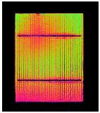
Topography of irregular surfaces
While nanoradian probe is available commercially,
the standard tool provides micro-radian range
reproducibility
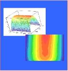
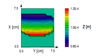
Example of measured mirror surface:
Example of measured surface of the mirror having radius of
about 90 m is shown Figures below. Tool has also data fitting
capability allowing user to calculate surface parameters and
residuals.
Tool allows user to fit wide variety of surface models, and
calculate residuals. Difference between the fitted and measured
surfaces – can be exported in a spread-sheet format.
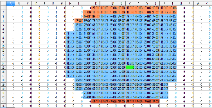
We observe quite satisfactory agreement for all central points
(blue points).
Wafer curvature and stress
For full report please contact sales@zebraoptical.com

| For more information, product application note, and brochure including detailed specification please fill information request form |
Please see short video demonstration.

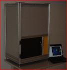
ZebraOptical Optoprofiler: Model X